
About
"Jiaxing AOSITE Photonics Technology Co.,Ltd. (hereinafter referred to as “OST Photonics”) is a high-technology company specialized in manufacturing and developing various of crystal material products. With more than twenty years experience, OST Photonics is committed to becoming the most professional manufacturer and supplier in the world. Our main products are as follows:• Scintillation crystal, encapsulated scintillator, pixellated array and scintillation detector for nuclear radiation detection.• Laser crystals, optics and components for laser system and applications.• IR windows and OEM optics for thermal imaging cameras and applications.• SAW/optical grade LiNbO3, LiTaO3, Quartz wafers and all types of crystal substrates for industrial and research applications.Our products are widely used in the laser systems, thermal imaging cameras, medical imaging systems, nuclear detection instruments, medical and biological equipments, defense and security, scientific research and aerospace.In the past few years, we have been cooperated closely with many scientific research centers, laboratories, universities and instrument manufacturers around the world, all our customers are satisfied with our products and services.Here at OST Photonics we value specialty, accountability and innovation. Our mission is to be your dependable partner to help you in growth." http://ostphotonics.com/
Home
Jiaxing AOSITE Photonics Technology Co.,Ltd. (OST Photonics) is a high-technology company specialized in manufacturing and developing various of crystal material products. Over the years, with reliable product quality, excellent service and rich experience in crystal processing and production, we are committed to becoming the most professional crystal products manufacturer and supplier in the world.
Contact
Hangzhou Branch: Room 1012, Chunhua Bussiness Center, No. 159, Hangbo Street, Shangcheng District, Hangzhou 310009, Zhejiang, China
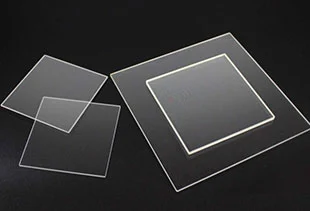
Optical Glass & Fused Silica Wafers
Compared with traditional glass lenses, the optical glass wafer from OST Photonics has the characteristics of higher surface quality, thinner size, more precise machining precision, and more stringent surface finish. Due to their excellent light transmittance, extremely low fluorescence intensity, extremely low expansion coefficient, strong thermal and impact resistance, excellent chemical stability, and excellent scratch resistance, optical glass wafers are widely used in CMOS, CCD sensors, integrated circuits or MEMS, communication and data processing, optics, electronic products, military, scientific research, and other high-tech products. If you want to know about optical glass types and want to buy optical glass wafers, please do not hesitate to contact OST Photonics, we are a professional glass wafer supplier.
What Is Fused Silica (Also Known As Fused Quartz)?
Fused silica is an amorphous (glassy) silica. It is a typical glass with a long-range disorder of its atomic structure. Fused silica is generally used as the main raw material for refractory materials, ceramic raw materials and glass raw materials, epoxy resin casting, electronic sealing materials, electric light sources, medical treatment, casting, and other industries. It is also an ideal filler for chemical industries such as paints and coatings.
What Are the Popular Applications for Optical Glass Wafers?
MEMS and electronics industry: In MEMS and electronics applications, optical glass wafers are used in the packaging of sensitive components because of their superior functionality and reliability, and stability in the face of harsh environments. Because of optical glass wafers have thermal stability and chemical resistance, glass can also be used as a carrier substrate.
Semiconductor: Optical glass wafers are used as carrier substrates in the production of semiconductor wafers, these optical glass wafers are made of finer materials that are easily bent or torn. Glass was chosen because of its superior chemical and thermal stability, and the potential for reuse can reduce the cost of some applications.
Biotechnology: Optical glass wafers can be used as glass substrates for a variety of biotechnology applications. Borosilicate glass is a ideal choice for medical devices with excellent resistance to high temperature and radiation, such as in X-ray equipment. Optical glass wafers are also used to produce microfluidic chips using nanoimprint lithography, in which glass acts as the substrate. Glass provides the clear optical transparency required for many biotechnology applications, making it a common choice for use as an overlay on devices made of silicon.
Integrated circuit (IC) packaging: Optical glass wafers are used in a variety of integrated circuit (IC) packaging applications, providing better performance and cost-effectiveness as substrates.
How Do Optical Glasses Work?
Optical glasses work by manipulating light to correct vision impairments such as farsightedness and nearsightedness. A plus/convex (+) lens, crafted from high-quality optical glass, corrects farsightedness by bending incoming light rays and moving the focal point forward, allowing the light to properly focus on the retina. On the other hand, a minus/concave (-) lens addresses nearsightedness by shifting the light’s focal point backward, ensuring it correctly focuses on the retina.
Optical glass is meticulously engineered to minimize impurities and maximize light transmission, making it essential for high-precision applications. Glass wafers, another form of optical glass, are used in various advanced technologies, including semiconductors and photonics.
OST Photonics, a leading optical glass manufacturer, specializes in producing these high-quality optical glass products. Their expertise ensures that the optical glasses and glass wafers they produce meet the stringent requirements of industries ranging from medical imaging to telecommunications. By offering advanced optical solutions, OST Photonics significantly enhances the performance and reliability of optical systems worldwide.
Why Use Borofloat 33 Glass Wafers(BF33 glass)?
Borofloat 33 (BF33) is often chosen by researchers for its durability and resistance to thermal shock. BF33 , which includes silica, has a very low coefficient of thermal expansion. It also has a much higher melting point, over 1500 degrees Fahrenheit, compared to other types of glass. BF33 is frequently used in research lab equipment as well as optical and lighting applications.
The Advantages of BF33 Glass:
Hypoallergenic
Outstanding Thermal Resistance
Exceptional High-Transparency
High Chemical Durability
Excellent Mechanical Strength
Lead Free
Other Popular Searches:
piezoelectric quartz single crystal
KDP nonlinear crystal
plastic scintillator material
CdWO4 scintillator
Lithium Niobate supplier
lithium tantalate wafers
single crystal quartz wafers
FAQS about Optical Glass & Fused Silica Wafers
What Are The Characteristics To Consider When Choosing Optical Glass?
Choosing optical glasses requires consideration of the optical, mechanical and thermal properties of the glass and how these factors will affect applications. Factors to consider are: transparency, uniformity, refractive index, dispersion, density, hardness and melting point.
What Is The Difference Between Optical Glass Wafers And Regular Glass Wafers?
Optical glass wafers and regular glass wafers differ primarily in their purity and light transmission capabilities. Optical glass wafers are meticulously engineered to minimize impurities and defects, allowing it to transmit light effectively even at significant thicknesses, such as 100 meters. In contrast, regular glass contains more impurities and structural inconsistencies, which hinder its ability to transmit light over long distances. This makes optical glass wafers essential for applications requiring precise light control, such as lenses and scientific instruments.
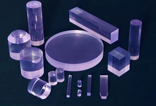
Plastic Scintillators
plastic scintillator material have the advantages of fast time response, low cost, high light output, and sensitivity to X-rays, gamma-rays, alpha-rays, beta-rays, and fast neutrons. These plastic scintillator materials also have excellent durability, and by mold and other methods, they can be made into almost any shape you want, including cast sheets, blocks, rods, cylinders, and thin films. Plastic scintillators are now widely used in a broad range of radiation detection applications.
OST Photonics can supply SPM100 light guide and various plastic scintillator materials for different applications: SP101 plastic scintillator for gamma-ray detection, SP102 plastic scintillator for beta- Ray detection, SP121 plastic scintillator for alpha-ray and beta-ray detection, SP122 plastic scintillator for low energy gamma-ray detection and SP123 plastic scintillator for alpha-ray detection. The SPM100 light guide is an optical transmission device made of PMMA material imported from Germany. If you want to know the plastic scintillator price and plastic scintillator properties or if you want to buy plastic scintillator, please feel free to contact OST Photonics, we are a professional plastic scintillator manufacturer.
Advantages of Plastic Scintillators
OST Photonics offers a wide range of plastic scintillator materials designed for various radiation detection applications. Here are some key advantages of using plastic scintillators:
Good Light Output: Plastic scintillator materials provide excellent light output, making them highly effective for detecting radiation.
Fast Time Response: With rapid response times, scintillating plastic is ideal for applications requiring quick detection and measurement.
Versatility: These plastic scintillator materials are suitable for a variety of industries, from medical imaging to nuclear safety.
Cost-Effective: When you buy plastic scintillators, you benefit from their affordability compared to other scintillator materials.
Durability: Plastic scintillators are robust and can withstand harsh environmental conditions.
Customizable: OST Photonics offers customizable options to meet specific needs, ensuring you get the right plastic scintillator properties for your application.
Whether you are looking to buy plastic scintillators or seeking information on plastic scintillator prices, OST Photonics has got you covered.
What Is a Plastic Scintillator Used For?
Plastic scintillators have a wide range of applications due to their exceptional properties. Here are some key uses:
Portal Vehicle Radiation Monitoring Systems: Plastic scintillator materials are ideal for detecting radiation in vehicles passing through security checkpoints.
Portable Radioactive Instruments: Their high sensitivity and fast time response make scintillating plastic perfect for handheld devices used in field measurements.
High Energy Physics Experiments: The reliable and accurate results provided by plastic scintillators are crucial for experiments in high energy physics.
Medical Imaging: The fast response time and good light output of plastic scintillators make them suitable for various medical imaging applications.
Environmental Monitoring: These materials are also used in devices that monitor environmental radiation levels.
Composition of Plastic Scintillator
(1)plastic matrix
The plastic matrix is a crucial component of plastic scintillators, accounting for over 97% of the material and having a significant impact on its physical and chemical properties. Aromatic compounds are the most common type of matrix used in plastic scintillators due to their necessary role in fluorescence absorption and emission processes. These aromatic matrices can be categorized into polystyrene, polyester, polysiloxane, polyepoxy resin, and polyvinyl alcohol. Polystyrene (PST) and polyvinyl toluene (PVT) are among the earliest matrices used with high detection efficiency. Non-aromatic matrices such as polymethyl methacrylate (PMMA), composed of carbon-oxygen double bonds and ester-bonded oxygen atoms, have weaker fluorescence intensity but better transparency than polystyrene. When used in combination with an aromatic solvent at a certain proportion, PMMA can improve both mechanical properties and transparency.
(2)scintillating material
The luminescence efficiency of the matrix in the plastic scintillator is very low, and when the scintillator is subjected to nuclear radiation (α, β, γ rays, etc.) or high-energy particles, if only the plastic matrix is used, most of the electron excitation energy will be released in non-radiative form and affect the detection efficiency. At the same time, the emission spectrum of the plastic matrix is primarily in the range of 300-350 nm. However, this emission wavelength is too short to match with ordinary photomultiplier tubes which have a low quantum efficiency in this band. Therefore, it becomes necessary to add scintillation materials to increase light yield in plastic scintillators. Scintillation materials can be divided into primary scintillation materials and wave shifting agents that should possess good solubility and temperature resistance (able to withstand temperatures between 100-170 °C), chemical stability (must coexist with all other components without being vulnerable to free radical attack during polymerization process), light resistance and low cost. Primary scintillation material refers to an aromatic compound which serves as the main luminous material with a mass fraction usually ranging from 0.3-4% and fluorescence emission wavelength between 350-400 nm. On the other hand, wave shifting agents are responsible for shifting maximum luminous wavelength towards a range that matches photomultiplier tubes; their mass fraction is lower than that of primary scintillation substance typically falling within 0.001-0.1wt %. Additionally, ultraviolet absorption spectrum of primary scintillation material should coincide with fluorescence spectrum of plastic matrix while ultraviolet absorption spectrum of wave shifting agent should match fluorescence spectrum of primary scintillation material so as to minimize energy loss and improve detection efficiency.
How Does A Plastic Scintillator Work?
A plastic scintillator works by converting ionizing radiation into visible light, which can then be detected and measured. When a plastic scintillator is exposed to ionizing radiation, electrons within the scintillating plastic become excited and move from their locked position in the valence band to the conduction band, where they are free to move around. This movement leaves an associated hole behind in the valence band. As the excited electrons return to their original state, they release energy in the form of photons, producing visible light.
Plastic scintillator materials are valued for their fast response time, durability, and ease of fabrication. Key plastic scintillator properties include high light output, good transparency, and the ability to be shaped into various forms for different applications.
OST Photonics, a premier manufacturer of scintillator materials, excels in producing top-tier plastic scintillators. Their cutting-edge materials find applications in diverse fields, including medical imaging and radiation detection, providing dependable and efficient performance. By delivering exceptional scintillating plastic solutions, OST Photonics significantly contributes to advancing the effectiveness of radiation detection systems globally.
FAQs of Plastic Scintillators
Is it possible to provide reflective and light shielding layers for plastic scintillator?
Yes, we are able to provide Aluminum foil as the reflective layer and black PVC material as the light shielding layer.
What regular sizes are available?
50 x 500 x 1000 mm/1200 mm, 50 x 700 x 1400 mm, 1200 x 500 x 84 mm, 1000 x 500 x 100 mm, 200 x 200 x 0.5 mm/1.0 mm, 300 x 300 x 0.5 mm/1.0 mm, D50 x 1000 mm/2000 mm etc.
Is it possible to provide PMT and electronics for the plastic scintillator?
Yes, we are able to provide different models of PMTs and electronics (voltage dividers, HV modules, pre-amplifiers, etc.) for the plastic scintillator upon requests.
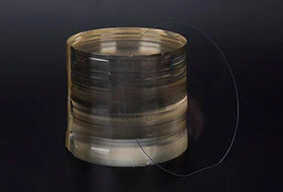
SAW & Optical Grade Lithium Niobate Wafers(LiNbO3 Wafers)
Lithium niobate (LiNbO3 or LN) crystal integrates piezoelectric, electro-optical, acoustic optical, photoelastic, nonlinear, photorefractive, and laser activity effects. In addition to its advantages of stable mechanical properties, good machinability, heat resistance, corrosion resistance, low price, easy to grow into large crystals, Lithium niobate (LiNbO3 or LN) crystal is the best photonic crystal material found so far. LiNbO3 crystal has a very broad market application value, so it is also called the "optical silicon" material of the photonic era, it is widely used in high-performance filters, electro-optical devices, holographic storage, 3D holographic display, nonlinear optical devices, optical quantum communication, and many other applications.
OST Photonics Lithium Niobate Supplier offers a variety of sizes and thicknesses of SAW&Optical grade Lithium Niobate (LiNbO3 or LN) wafers, with diameters ranging from 2 inches to 8 inches, the thickness can be customized according to your requirements (generally above 0.18 mm). The orientations can be X/Y/Z/Y41/Y64/Y128/YZ/YX or customized. Congruent lithium niobate (CLN), near-stoichiometric lithium niobate (SLN), pyroelectric free black linbo3 wafers and Tm/Pr/Er/Fe/MgO doped LiNbO3 wafers are also available. If you want to know the (LiNbO3 wafer or LN) lithium niobate wafer price and more information about wafers and substrates, please do not hesitate to contact OST Photonics Lithium Niobate Supplier, we are a professional lithium niobate wafer supplier.
Specifications of The lithium niobate wafers(LiNbO3 Wafers)
Other specifications are available on request
What Is The Difference Between SAW Grade LiNbO3 Wafers and Optical Grade LiNbO3 Wafers?
Optical grade lithium niobate is a low-strain, impurity-free crystal material grown from the best raw materials at a relatively slow growth rate and is commonly used in optical applications that require the highest quality. Optical grade lithium niobate wafers are widely used in optical devices with high-performance requirements.
SAW grade lithium niobate is mainly used for surface acoustic wave applications, and its growth raw material is second only to optical grade growth raw material, with a faster growth rate than optical grade lithium niobate, which facilitates mass production and cost-effectiveness.
In general, these grades of lithium niobate differ slightly in terms of material quality and usage, with optical grade lithium niobate considered to be of the highest quality while SAW grade lithium niobate has a relatively lower price.
Key Characteristics of Lithium Niobate Wafers(LiNbO3 Wafers)
The main characteristics of lithium niobate wafers are their excellent electrical properties and thermal stability.
Firstly, lithium niobate wafers have a high dielectric constant and low loss factor, which makes them widely used in microwave devices, surface acoustic wave filters, and other fields.
Secondly, lithium niobate wafers also exhibit good piezoelectric effect and transparency, playing an important role in ultrasonic transducers, optical modulators, and other devices.
Additionally, lithium niobate wafers possess excellent thermal stability as they can maintain structural integrity and mechanical strength even in high-temperature environments without being significantly affected by thermal expansion. This widespread usage includes applications such as high-temperature sensors and ceramic heating elements.
Furthermore, apart from the aforementioned characteristics, lithium niobate wafers demonstrate good chemical stability and biocompatibility. They exhibit resistance to various chemicals without causing allergies or toxic side effects when in contact with human tissue.
Therefore, within the medical field specifically, lithium niobate wafers find extensive use in artificial joints and dental repair materials among others. In summary, due to their exceptional electrical properties along with thermal stability as well as chemical stability and biocompatibility features; lithium niobate wafers have become indispensable materials across numerous fields while still holding significant potential for future development.
Applications of The Lithium Niobate Wafers(LiNbO3 Wafers)
Lithium niobate wafers are widely used.
Firstly, they play an important role in the field of electronics. Lithium niobate wafers can be utilized to manufacture high-performance capacitors and sensors, which are crucial in industries such as communications, computers, and automobiles.
Secondly, in the field of optics, lithium niobate wafers also hold significant importance as they can be applied to laser technology, optical fiber communication, and optical instruments to provide clearer and more accurate image and data transmission methods.
Additionally, lithium niobate wafers find applications in the medical field for manufacturing artificial heart pacemakers, biosensors, and other medical devices. Apart from these fields mentioned above, lithium niobate wafers have numerous other applications such as energy storage systems including solar panels etc., aerospace industry including satellite communication systems and navigation equipment etc., environmental protection by utilizing their special properties for developing new pollution control technologies.
In conclusion, due to their excellent physical and chemical properties along with wide adaptability across various industries there is a growing demand for lithium niobate wafers; furthermore with continuous scientific progress and innovation it is anticipated that more novel applications will emerge in the future.
FAQS about SAW&Optical Grade Lithium Niobate Wafers
What Is The Pyroelectric Free Black LiNbO3 Wafers?
We use reduction technique to produce pyroelectric free black LiNbO3 wafers, which has a high ability to neutralize charges even if the electric potential occurs instantaneously. The pyroelectric effect of black LiNbO3 wafers is almost eliminated and the transmittance is significantly reduced. The piezoelectric properties of black lithium niobate wafers are no different from those of standard wafers. Therefore, black reduced lithium niobate wafers are widely used to produce higher frequency surface acoustic wave devices.
What Devices Can LiNbO3 Wafers Be Used To Manufacture?
LiNbO3 wafers can be used to manufacture Q-switching devices, high-performance gyroscope, accelerators and accelerometer sensors, MEMS devices, surfaced acoustic devices and so on.